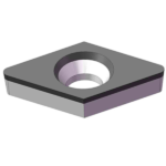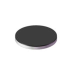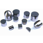
CVD Diamond Heat Sink Plates & Thermal Spreaders
Request a Quote
Enter the quantity you need and add to your quote list for pricing inquiries.
Description

The Ultimate Thermal Management Solution for Next-Gen High-Power Electronics
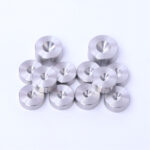
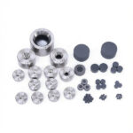
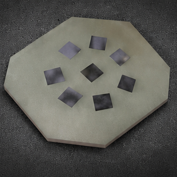
Through advanced Chemical Vapor Deposition (CVD) synthesis under rigorous microwave plasma (MPCVD) parameter control, Uking Diamond delivers polycrystalline diamond heat sinks with premium isotropic thermal conductivity surpassing 1200 to 2000 W/m·K.
Engineered to eliminate localized hotspots and thermal run-away, our micro-discs and submounts serve as the critical foundation for high-power optoelectronics, wide-bandgap semiconductors (GaN/SiC), RF microwave amplifiers, and aerospace radar modules.
PRODUCT SPECIFICATIONS
| Thickness(μm) | Customizable upon request | Flexural Strength (MPa) | 450-1100 |
| Density(g/cm³) | 3.3216 | Young’s Modulus (GPa) | 1000-1100 |
| Thermal Conductivity (W/m-K) | TC1200, TC1500, TC1800, TC2000 | Dielectric Constant (1MHz) | 5.68 |
| Thermal Diffusivity(cm³/s) | 6.6, 8.2, 9.9 | Dielectric Loss(1MHz) | 6.2×10⁻⁸ |
| Thermal Expansion Coefficient (RT-700°C) (10-6/K) | 3.1962 | Volume Resistivity(25″C,Q-cm) | 2.95×10¹³ |
| Vickers Hardness | >10 | BreakdownVoltage(V/mA) | ≥11kV/mm |
Laser-Ready Surface Roughness: Front-side specialized polishing down to Ra < 2nm ensuring atomic-level intimacy and zero thermal contact resistance TCR during eutectic bonding or sputtering. Back-side chemical etched or polished up to Ra 30–100nm matching custom dielectric metallization layout.
Total Thickness Variation:
Strictly calibrated TTV < 5μm (across 2-inch wafers) to guarantee uniform pressure distribution during device integration, significantly increasing package yield rates.
DIMENSIONS & SURFACE CHARACTERISTICS
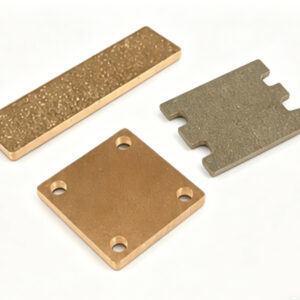
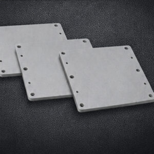
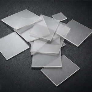
| Standard Sizes ● Optical window flatness(front): Ra<30nm (< 2nm customizable) ● Back surface roughness (front):30-100nm (customizable)(measured area 12Sx125μm) ● Back surfaceroughness(back):30nm-2um (customizable)(measured area 125×125μm) ● TTV:50μm(2 inch) customizable Thickness:<300um(2 inch) customizable |  | Shape Options Available in multiple shapes:  ●Custom shapes and sizes are availablle according to customer drawings. |
High-Power Laser Diodes (LD) & Modules
Prevents wavelength drift and power degradation in multi-watt industrial laser bars by facilitating ultra-fast lateral heat spreading directly beneath the cavity facet.
Wide-Bandgap Semiconductors (GaN on Diamond / SiC)
- Unlocks the true power density potential of Gallium Nitride (GaN) and Silicon Carbide (SiC) RF power amplifiers by dropping junction temperatures by up to 50 ℃
- RF, Microwave & 5G/6G Infrastructure
- Enhances signal integrity and Mean Time Between Failures (MTBF) in solid-state power amplifiers (SSPA) operating under extreme continuous wave (CW) conditions.
· Aerospace & High-Reliability Electronics
- Delivers radiation-hardened, corrosion-resistant thermal defense matrices that endure severe thermal shock profiles in deep-space and defense missions.

Eliminate Downtime & Submount Failures. Unlock Your Engineering Validation Pass.
Every high-performance CVD diamond thermal spreader is born in our state-of-the-art microwave plasma synthesis grid, verified by non-destructive thermal diffusivity testing. Because premium diamond wafers represent a high-value engineering investment, we do not distribute unchecked free handouts. We focus on absolute technical alignment.
Ready to validate the performance leap on your assembly line? Contact our global engineering desk today with your standard configuration requirements (Square, Rectangle, Round, Hexagon, or Special Shapes) and your target thermal conductivity grade (TC1200-TC2000).
While we do not offer free samples, we will wave all metallization engineering fees and custom cutting design charges for verified qualified corporate clients. Secure an Engineering Trial Pass today to receive your evaluation batch at factory-direct wholesale cost, with 100% of the sample evaluation fee fully credited back to your account upon your first bulk commercial order.